Shenzhen Vencore Electronics Co., Ltd.
Tel: 0755-27267961
Email: sales@vencorepcb.com
Website: www.vencorepcb.com
Address : Buildings 221 and 226, Dazheng Technology Park, Jiangbian Industrial Road 6, Songgang Street, Bao'an District, Shenzhen
Building 2, No. 119 Changmao Road, Changzhen Community, Yutang Street, Guangming District, Shenzhen
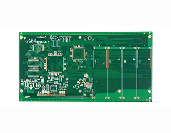
The surface treatment methods used by circuit board manufacturers in proofing are different, and each has its own unique characteristics. Taking chemical silver as an example, lead-free soldering and smt are recommended. Especially for fine circuit boards, the effect is better. On top of that, the use of chemical silver for surface treatment significantly reduces overall cost and cost. Let’s take a look at several common surface treatment methods for circuit boards with Xiaobian.
HASL hot air leveling (ie spray tin)
Tin spraying is a common processing method in the early stage of PCB proofing. Now it is divided into lead spray tin and lead-free spray tin. The advantages of tin spraying: after the PCB is completed, the copper surface is completely wet (the tin is completely covered before soldering), suitable for lead-free soldering, the process is mature, the cost is low, suitable for visual inspection and electrical testing, and it is also a high-quality and reliable PCB board proofing processing one of the methods.

chemical nickel gold
Nickel gold is a surface treatment process for PCB board sampling. Remember: the nickel layer is a nickel phosphorous alloy layer. According to the phosphorus content, it is divided into high phosphorus nickel and medium phosphorus nickel. The applications are different, so I will not introduce them one by one here. the difference. Advantages of nickel-gold: suitable for lead-free soldering; very flat surface, suitable for SMT, suitable for electrical testing, suitable for switch contact design, suitable for aluminum wire binding, suitable for thick plates, strong resistance to environmental attacks.
Electroplated nickel gold
Electroplated nickel gold is divided into "hard gold" and "soft gold". Hard gold (eg: gold-cobalt alloy) is commonly used on gold fingers (contact connection design), and soft gold is pure gold. Nickel and gold electroplating is widely used for IC substrates such as PBGA. It is mainly bonded with gold and copper wires, but IC substrates are suitable for electroplating. Bonded gold finger areas require additional plated wires. The advantage of electroplated nickel-gold pcb board proofing is that it is suitable for contact switch design and gold wire bonding, and is suitable for electrical testing.
Nickel Palladium
Nickel-palladium-gold is now gradually used in the field of PCB proofing, and was used more in semiconductors before. Suitable for bonding of gold and aluminum wires. The advantage of proofing with nickel-palladium-gold pcb board is the application on IC carrier board, which is suitable for gold wire bonding, aluminum wire bonding, and also suitable for lead-free soldering. Compared with ENIG, there is no nickel corrosion (black disk) problem, the cost is cheaper than ENIG and electro-nickel-gold, and it is suitable for various surface treatment processes and on-board.
The above are the surface treatment methods commonly used by circuit board manufacturers in the proofing process. Each has its own advantages, and the scope of use is also different. Specific problems need to be dealt with in detail. If you have any other questions, please contact us~

Copyright © Shenzhen Vencore Electronics Co., Ltd. Number:粤ICP备2021150348号